| CPC H04N 17/002 (2013.01) [H04N 7/183 (2013.01); H04N 25/702 (2023.01); H04N 25/745 (2023.01); H04N 25/75 (2023.01)] | 13 Claims |
|
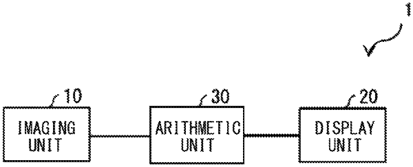
1. An imaging device comprising:
a pixel array including a plurality of pixels;
a scanning control section that controls scanning of the plurality of pixels;
a readout control section that controls reading of the plurality of pixels;
a first waveform generation part that generates a plurality of control signals for controlling of at least one of the scanning control section or the readout control section;
a second waveform generation part that generates a plurality of reference signals; and
a failure detection section that detects a failure of the first waveform generation part or the second waveform generation part on a basis of comparison between the plurality of control signals and the plurality of reference signals, wherein
the first waveform generation part includes a first register section that outputs a plurality of set values, and a first timing generation section that outputs the plurality of control signals on a basis of the plurality of set values, and
the second waveform generation part includes a second timing generation section that outputs the plurality of reference signals on a basis of the plurality of set values.
|