| CPC H04N 1/52 (2013.01) [G06K 15/102 (2013.01); H04N 1/0005 (2013.01); H04N 1/00023 (2013.01); H04N 1/00037 (2013.01); H04N 1/00084 (2013.01)] | 20 Claims |
|
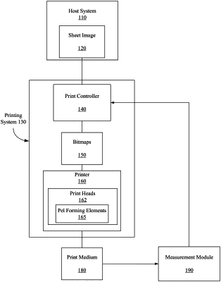
1. A system comprising:
at least one physical memory device to store compensation logic; and
one or more processors coupled with the at least one physical memory device to execute the compensation logic to:
generate transfer functions for each of a plurality of color planes to compensate for non-functioning pel forming elements, wherein the transfer functions are generated based on ink deposition functions for groups of pel forming elements including functioning pel forming elements and the non-functioning pel forming elements, wherein the transfer functions transform input digital counts, and wherein the ink deposition functions represent output ink amount versus input digital count.
|