| CPC H03H 9/02897 (2013.01) [H01L 24/13 (2013.01); H01L 25/18 (2013.01); H03H 9/1085 (2013.01); H01L 25/0655 (2013.01); H01L 25/50 (2013.01); H01L 2224/131 (2013.01); H01L 2224/13139 (2013.01); H01L 2224/13144 (2013.01); H01L 2224/13155 (2013.01); H01L 2224/16227 (2013.01); H01L 2224/81205 (2013.01); H01L 2224/81815 (2013.01); H01L 2924/15313 (2013.01); H01L 2924/35121 (2013.01); H03H 9/059 (2013.01); H03H 9/0542 (2013.01)] | 20 Claims |
|
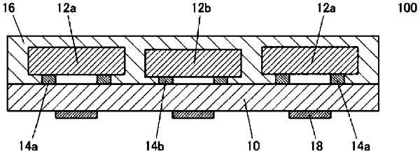
1. An electronic component comprising:
a package substrate extending in a longitudinal direction; and
a plurality of chip components disposed along the longitudinal direction of the package substrate and each connected to the package substrate by a bump; wherein
a height of any bump connecting at least one chip component disposed at an end portion in the longitudinal direction of the package substrate among the plurality of chip components and the package substrate is greater than a height of any bump connecting at least one chip component disposed inward relative to the end portion in the longitudinal direction of the package substrate among the plurality of chip components and the package substrate; and
in a top view of the package substrate, the plurality of chip components are spaced apart from one another along the longitudinal direction of the package substrate.
|