| CPC H03F 3/245 (2013.01) [H03F 3/195 (2013.01); H03F 2200/102 (2013.01); H03F 2200/171 (2013.01); H03F 2200/451 (2013.01); H03F 2200/537 (2013.01)] | 10 Claims |
|
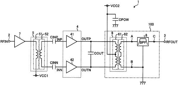
1. A power amplifier circuit having an input node to which a high-frequency signal is input and an output node from which an amplified high-frequency signal is output, the high-frequency signal being amplified by a differential amplifier circuit, the power amplifier circuit comprising:
a balun transformer comprising an input-side winding that is connected between differential outputs of the differential amplifier circuit, and an output-side winding that is coupled to the input-side winding via an electromagnetic field and that has a first end connected to a reference potential;
a capacitive element between a second end of the output-side winding and the output node; and
a band pass filter between the second end of the output-side winding and the output node, the band pass filter comprising the capacitive element,
wherein the input-side winding has a substantially centered tap, and
wherein a power-supply voltage is supplied to the substantially centered tap.
|