| CPC H03F 1/0233 (2013.01) [H03F 1/3211 (2013.01); H03F 3/213 (2013.01); H03F 3/45264 (2013.01)] | 20 Claims |
|
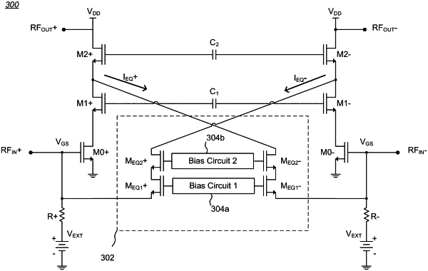
1. A differential amplifier, including:
(a) a first main field-effect transistor (FET) including a gate configured to receive a first input signal, a drain providing a first amplified output signal, and a source coupled to circuit ground;
(b) a second main FET including a gate configured to receive a second input signal, a drain providing a second amplified output signal, and a source coupled to circuit ground; and
(c) an equalization circuit coupled to the respective gates and drains of the first and second main FETs and configured to generate an equalization voltage that alters a bias voltage to the gates of the respective first and second main FETs in proportion to a power level present at the respective drains of the second and first main FETs, wherein the equalization circuit includes:
(1) a first equalization subcircuit including a stack of n series-coupled transistors, wherein n≥1, the stack of n series-coupled transistors of the first equalization subcircuit having a first transistor having a source coupled to the gate of the first main FET and a last transistor having a drain coupled to the drain of the second main FET; and
(2) a second equalization subcircuit including a stack of n series-coupled transistors, wherein n≥1, the stack of n series-coupled transistors of the second equalization subcircuit having a first transistor having a source coupled to the gate of the second main FET and a last transistor having a drain coupled to the drain of the first main FET.
|