| CPC H02M 1/08 (2013.01) [H02M 1/38 (2013.01); H02M 3/157 (2013.01); H02M 3/158 (2013.01); H03K 17/08 (2013.01); H03K 17/284 (2013.01); H03K 19/20 (2013.01); H03K 2017/0806 (2013.01)] | 16 Claims |
|
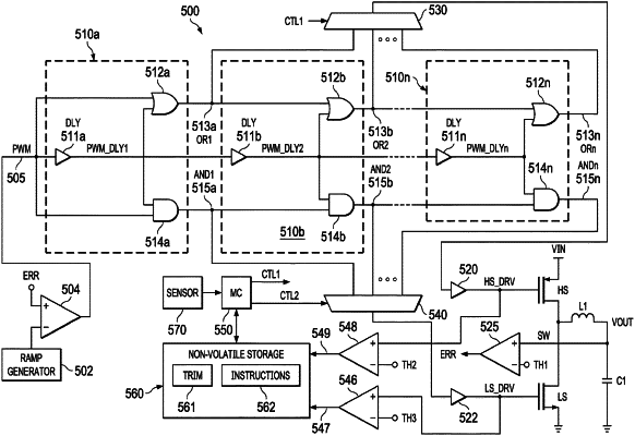
1. A circuit, comprising:
a first gate control circuit including a first time delay element, a first logic gate, and a second logic gate, the first time delay element including an output, and wherein the first logic gate includes a first output and the second logic gate includes a second output;
a second gate control circuit including a second time delay element, a third logic gate, and a fourth logic gate, wherein the second time delay element includes an input coupled to the output of the first time delay element, the second time delay element includes an output, the third logic gate includes a third output, and the fourth logic gate includes a fourth output;
a first gate driver coupled to one of the first or third outputs;
a first selection circuit coupled to the first and third outputs;
a second gate driver coupled to one of the second or fourth outputs; and
a second selection circuit coupled to the second and fourth outputs.
|