| CPC H02M 1/08 (2013.01) [H02M 1/0006 (2021.05); H02M 3/158 (2013.01)] | 20 Claims |
|
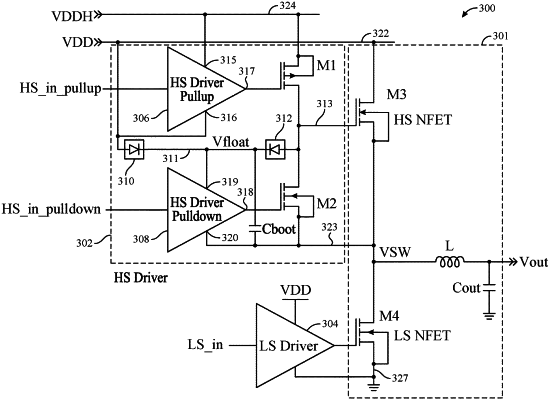
1. A gate driver for a switching transistor of a power supply circuit, the gate driver comprising:
a first power supply rail;
a reference rail;
an output node for coupling to a control input of the switching transistor;
a floating supply node;
a pulldown transistor having a drain coupled to the output node of the gate driver and having a source coupled to the reference rail; and
a pulldown logic buffer having a first power supply input coupled to the floating supply node, having a second power supply input coupled to the reference rail, and having an output coupled to a gate of the pulldown transistor, wherein the floating supply node is configured to selectively receive power from the first power supply rail and the output node of the gate driver.
|