US 11,817,698 B2
Battery management circuit, power storage device, and electric device
Kei Takahashi, Kanagawa (JP); Koji Kusunoki, Kanagawa (JP); Kouhei Toyotaka, Kanagawa (JP); and Kazunori Watanabe, Tokyo (JP)
Assigned to Semiconductor Energy Laboratory Co., Ltd., Kanagawa-ken (JP)
Appl. No. 17/256,667
Filed by SEMICONDUCTOR ENERGY LABORATORY CO., LTD., Atsugi (JP)
PCT Filed Jun. 25, 2019, PCT No. PCT/IB2019/055319
§ 371(c)(1), (2) Date Dec. 29, 2020,
PCT Pub. No. WO2020/008297, PCT Pub. Date Jan. 9, 2020.
Claims priority of application No. 2018-128702 (JP), filed on Jul. 6, 2018.
Prior Publication US 2021/0376646 A1, Dec. 2, 2021
Int. Cl. H02J 7/00 (2006.01); G01R 31/396 (2019.01); G01R 31/3835 (2019.01); H01L 29/786 (2006.01)
CPC H02J 7/007182 (2020.01) [G01R 31/3835 (2019.01); G01R 31/396 (2019.01); H02J 7/0048 (2020.01); H01L 29/7869 (2013.01)] 7 Claims
OG exemplary drawing
 
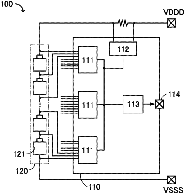
1. A battery management circuit of a battery cell comprising:
a voltage monitor circuit,
wherein the voltage monitor circuit includes a multiplexer and a buffer circuit for outputting a signal for controlling the multiplexer,
wherein the multiplexer and the buffer circuit each include an n-channel transistor, and
wherein the n-channel transistor is a transistor including an oxide semiconductor in a channel formation region.