| CPC H01Q 9/045 (2013.01) [H01Q 1/48 (2013.01); H01Q 19/005 (2013.01); H01Q 9/0435 (2013.01); H01Q 21/065 (2013.01)] | 18 Claims |
|
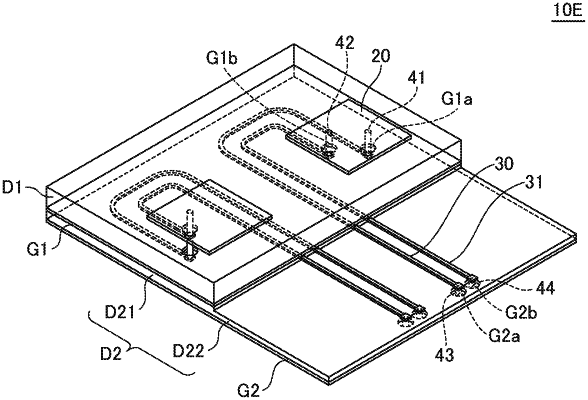
1. A patch antenna comprising:
a dielectric layer in which a patch conductor and a signal line are provided;
a feed conductor provided perpendicularly to the patch conductor so as to connect a feed point for the patch conductor;
a first ground pattern provided between the patch conductor and the signal thief line in a first direction; and
a second ground pattern provided on an opposite side to the first ground pattern with respect to the signal line,
wherein the dielectric layer has a first region and a second region having a thickness in the first direction smaller than that of the first region,
wherein the first and second regions are arranged in a second direction perpendicular to the first direction,
wherein the patch conductor is provided on the first region of the dielectric layer, and
wherein the first signal line is formed over the first and second regions of the dielectric layer.
|