| CPC H01Q 1/243 (2013.01) [H04M 1/0266 (2013.01); H04M 1/0277 (2013.01)] | 16 Claims |
|
1. An electronic device comprising:
a display panel comprising a first surface facing a first direction and a second surface facing a second direction;
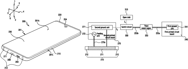
a first printed circuit board configured to be positioned in the second direction of the display panel and to comprise a first ground unit;
a bracket comprising a first structure which forms a side surface of the electronic device and a second structure which forms a space in which electronic components are mounted, wherein the first structure of the bracket comprises a first metal region operating as a radiator and insulation regions positioned at both ends of the first metal region, and the second structure of the bracket comprises a second metal region, a first non-metal region, and a third metal region extending through one region of the first non-metal region;
a wireless communication circuit which is electrically connected to the first metal region and is configured to transmit or receive at least one signal having a designated frequency;
a second printed circuit board comprising a second ground unit;
a switch circuit configured to electrically connect the third metal region to the second ground unit or an open stub;
at least one processor configured to be electrically connected to the switch circuit and to control a connection state of the switch circuit; and
a memory in which connection state information of the switch circuit corresponding to a frequency band of the at least one signal is stored,
wherein the first metal region is electrically connected to the second printed circuit board,
wherein the third metal region is electrically connected to the first ground unit and the second ground unit, and
wherein the at least one processor is further configured to control the connection state of the switch circuit based on the connection state information of the switch circuit corresponding to the frequency band of the at least one signal.
|