| CPC H01L 33/62 (2013.01) [H01L 25/0753 (2013.01); H01L 25/167 (2013.01); H01L 33/0093 (2020.05); H01L 33/52 (2013.01); H01L 33/0095 (2013.01); H01L 2933/005 (2013.01); H01L 2933/0066 (2013.01)] | 16 Claims |
|
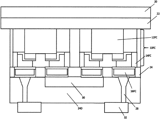
1. A method for making electronic device arrays comprising:
providing a plurality of separate electronic devices;
providing a carrier substrate and a temporary substrate attached to the carrier substrate, the carrier substrate configured as a support substrate for supporting the electronic devices and the temporary substrate configured as an attaching substrate for attaching the electronic devices to the support substrate;
attaching the electronic devices to the temporary substrate;
forming one or more insulator layers on the electronic devices while attached to the temporary substrate;
forming one or more metal layers configured to electrically connect the electronic devices to form a desired circuitry; and
separating the electronic devices along with the metal layers and the insulator layers from the carrier substrate and the temporary substrate.
|