| CPC H01L 33/505 (2013.01) [H01L 33/60 (2013.01); H10K 50/852 (2023.02); H10K 59/10 (2023.02); H10K 59/38 (2023.02); H01L 2933/0041 (2013.01); H10K 50/844 (2023.02); H10K 59/124 (2023.02); H10K 59/352 (2023.02); H10K 71/00 (2023.02); H10K 2102/351 (2023.02)] | 6 Claims |
|
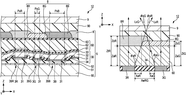
1. An electro optical device comprising:
an electrode;
a first pixel electrode;
a second pixel electrode disposed next to the first pixel electrode in plan view;
a light-emitting function layer disposed in a first layer between the electrode and the first and second pixel electrodes;
a first color filter disposed corresponding to the first pixel electrode;
a second color filter disposed corresponding to the second pixel electrode; and
a transparent layer disposed in a second layer between the electrode and the first and second color filters, wherein
in plan view, a distance between a first region where the first pixel electrode and the light-emitting functional layer are in contact with each other and a second region where the second pixel electrode and the light-emitting functional layer are in contact with each other is 1.5 μm or less, and a sum of a first thickness of the first color filter and a second thickness between the first color filter and the electrode is 8 times or less the distance.
|