| CPC H01L 33/505 (2013.01) [H01L 25/0753 (2013.01); H01L 27/156 (2013.01); H01L 33/44 (2013.01); H01L 33/504 (2013.01); H01L 33/62 (2013.01); H01L 33/0093 (2020.05); H01L 33/10 (2013.01); H01L 33/20 (2013.01); H01L 33/46 (2013.01); H01L 2933/0025 (2013.01); H01L 2933/0041 (2013.01); H01L 2933/0058 (2013.01); H01L 2933/0066 (2013.01)] | 20 Claims |
|
1. A light emitting diode (LED) array comprising:
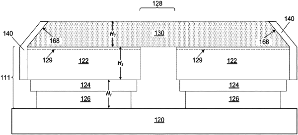
a first pixel comprising a first epitaxial layer and a second pixel comprising a second epitaxial layer, each of the first epitaxial layer and the second epitaxial layer emitting light in operation and comprising a p-type region, an active region on the p-type region, and an n-type region on the active region;
a continuous wavelength converting layer on the first pixel and the second pixel and extending between the first pixel and the second pixel, the continuous wavelength converting layer comprising a first surface on and in direct contact with the first epitaxial layer and the second epitaxial layer and having a width that is greater than a sum of a width of the first epitaxial layer and a width of the second epitaxial layer, a second surface parallel to the first surface having a width that is less than the width of the first surface, and first angled sidewalls; and
a first thin conformal layer on the first angled sidewalls of the continuous wavelength converting layer, and on sidewalls of the first epitaxial layer and the second epitaxial layer, that leaves the emission surface of the continuous wavelength converting layer exposed.
|