| CPC H01L 33/30 (2013.01) [H01L 33/0066 (2013.01); H01L 33/04 (2013.01); H01L 33/58 (2013.01)] | 11 Claims |
|
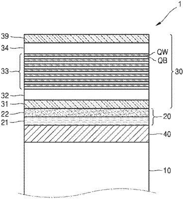
1. An optical device comprising:
a substrate;
a lattice matching layer directly contacting the substrate;
a multilayered GaAs structure directly contacting the lattice matching layer; and
an optical structure layer on the multilayered GaAs structure, the optical structure layer comprising a Group III-V compound semiconductor material,
wherein the multilayered GaAs structure comprises a first GaAs layer and a second GaAs layer stacked on the first GaAs layer, and
wherein the first GaAs layer has a density higher than a density of the second GaAs layer.
|