US 11,817,520 B2
Method for manufacturing stacked thin film, method for manufacturing solar cell, and method for manufacturing solar cell module
Soichiro Shibasaki, Nerima (JP); Yuya Honishi, Saitama (JP); Mutsuki Yamazaki, Yokohama (JP); Naoyuki Nakagawa, Setagaya (JP); Sara Yoshio, Yokohama (JP); Yoshiko Hiraoka, Kawasaki (JP); and Kazushige Yamamoto, Yokohama (JP)
Assigned to KABUSHIKI KAISHA TOSHIBA, Tokyo (JP); and TOSHIBA ENERGY SYSTEMS & SOLUTIONS CORPORATION, Kawasaki (JP)
Filed by KABUSHIKI KAISHA TOSHIBA, Tokyo (JP); and TOSHIBA ENERGY SYSTEMS & SOLUTIONS CORPORATION, Kawasaki (JP)
Filed on Sep. 9, 2020, as Appl. No. 17/015,490.
Application 17/015,490 is a continuation of application No. PCT/JP2020/008386, filed on Feb. 28, 2020.
Claims priority of application No. 2019-036209 (JP), filed on Feb. 28, 2019; application No. 2019-111030 (JP), filed on Jun. 14, 2019; and application No. 2020-033237 (JP), filed on Feb. 28, 2020.
Prior Publication US 2021/0013360 A1, Jan. 14, 2021
Int. Cl. H01L 31/18 (2006.01); H01L 31/046 (2014.01); H01L 31/076 (2012.01)
CPC H01L 31/18 (2013.01) [H01L 31/046 (2014.12); H01L 31/076 (2013.01)] 8 Claims
OG exemplary drawing
 
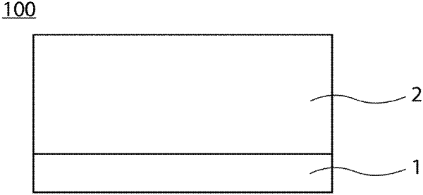
1. A method for manufacturing a stacked thin film, comprising:
forming a photoelectric conversion layer on a first transparent electrode by sputtering using a target mainly composed of copper in an atmosphere at an oxygen partial pressure in a range of 0.01 [Pa] or more and 4.8 [Pa] or less, wherein
the oxygen partial pressure of the sputtering is in the above range, and 0.5×d [Pa] or more and 1.5×d [Pa] or less when a deposition rate is d [μm/min], in formation of the photoelectric conversion layer, and
a sputtering temperature is 300° C. or more and 600° C. or less, in formation of the photoelectric conversion layer.