| CPC H01L 31/077 (2013.01) [H01L 31/202 (2013.01)] | 20 Claims |
|
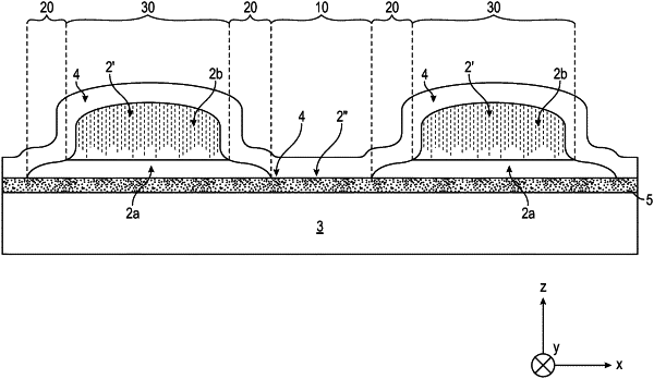
1. A photovoltaic device being an interdigitated back contact photovoltaic device comprising:
a silicon-based substrate being of p-type or n-type doping and having a first face defining a X-Y plane;
an intrinsic amorphous silicon layer a-Si:H(i) situated on said first face;
a first patterned silicon layer situated on said intrinsic layer, said first silicon layer being of p-type or n-type doping,
said first patterned silicon layer comprising interstices between charge collection portions, said charge collection portions comprising each second portions of an at least partially nano-crystalline silicon layer at their side away from said silicon-based substrate;
a second nano-crystalline silicon layer being situated on said charge collection portions, and on said interstices, and having another type of doping than the doping type of said patterned silicon layer,
wherein
said charge collection portions comprise each an amorphous layer portion situated between said intrinsic layer and said second portions, said amorphous layer portions having, in at least one of its cross sections parallel to said X-Y plane, and in any radial direction, a largest width that is greater than any width of said second portions, said amorphous layer portions and said second portions being basically centered to each other.
|