| CPC H01L 29/78696 (2013.01) [G06F 3/044 (2013.01); G06F 3/0412 (2013.01); H01L 21/02554 (2013.01); H01L 21/02565 (2013.01); H01L 21/02631 (2013.01); H01L 27/0296 (2013.01); H01L 27/127 (2013.01); H01L 27/1225 (2013.01); H01L 27/1259 (2013.01); H01L 29/24 (2013.01); H01L 29/66969 (2013.01); H01L 29/7869 (2013.01); H01L 29/78606 (2013.01); H01L 29/78648 (2013.01); G02F 1/1333 (2013.01); G02F 1/1368 (2013.01); G02F 1/13338 (2013.01); G02F 1/13685 (2021.01); H10K 59/1213 (2023.02)] | 15 Claims |
|
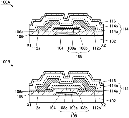
1. A method for manufacturing a semiconductor device comprising the steps of:
forming a gate electrode;
forming a first insulating layer over the gate electrode;
adding oxygen in a vicinity of a surface of the first insulating layer;
forming a metal oxide layer over the first insulating layer;
forming a pair of electrodes over the metal oxide layer; and
forming a second insulating layer over the pair of electrodes,
wherein the step of forming the metal oxide layer is divided into a first step and a second step to deposit the metal oxide layer in vacuum through the first step and the second step conducted continuously,
wherein the first step is conducted before the second step,
wherein the second step has a higher flow ratio of oxygen in a whole deposition gas than the first step,
wherein the second insulating layer comprises a first region and a second region,
wherein the first region comprises a region in contact with the metal oxide layer,
wherein the second region comprises a region containing more nitrogen than the first region and comprises a region containing more excess oxygen than the first region,
wherein the metal oxide layer has at least a concentration gradient of oxygen in a thickness direction, and
wherein the concentration gradient becomes high on a first region side and on a first insulating layer side.
|
|
2. The method for manufacturing a semiconductor device according to claim 1, further comprising the step of forming a third insulating layer over the second insulating layer,
wherein the third insulating layer comprises silicon nitride.
|