US 11,817,506 B2
Semiconductor device and manufacturing method thereof
Shunpei Yamazaki, Setagaya (JP); Junichiro Sakata, Atsugi (JP); and Jun Koyama, Sagamihara (JP)
Assigned to Semiconductor Energy Laboratory Co., Ltd., Kanagawa-ken (JP)
Filed by Semiconductor Energy Laboratory Co., Ltd., Atsugi (JP)
Filed on Jul. 6, 2021, as Appl. No. 17/367,689.
Application 17/367,689 is a continuation of application No. 16/789,872, filed on Feb. 13, 2020, abandoned.
Application 16/789,872 is a continuation of application No. 15/651,251, filed on Jul. 17, 2017, abandoned.
Application 15/651,251 is a continuation of application No. 14/849,928, filed on Sep. 10, 2015, granted, now 9,711,651, issued on Jul. 18, 2017.
Application 14/849,928 is a continuation of application No. 13/104,546, filed on May 10, 2011, granted, now 9,136,390, issued on Sep. 15, 2015.
Application 13/104,546 is a continuation of application No. 12/646,085, filed on Dec. 23, 2009, granted, now 8,222,092, issued on Jul. 17, 2012.
Claims priority of application No. 2008-333788 (JP), filed on Dec. 26, 2008.
Prior Publication US 2021/0336060 A1, Oct. 28, 2021
Int. Cl. H01L 29/786 (2006.01); H01L 27/12 (2006.01); H01L 29/66 (2006.01); H01L 29/24 (2006.01); H01L 21/02 (2006.01)
CPC H01L 29/7869 (2013.01) [H01L 27/124 (2013.01); H01L 27/1225 (2013.01); H01L 29/24 (2013.01); H01L 29/66969 (2013.01); H01L 29/78696 (2013.01); H01L 21/02554 (2013.01); H01L 21/02565 (2013.01); H01L 21/02631 (2013.01)] 13 Claims
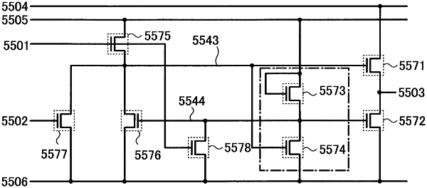
OG exemplary drawing
 
1. A semiconductor device comprising a transistor comprising:
a first metal oxide layer over a gate electrode;
a second metal oxide layer on the first metal oxide layer;
a third metal oxide layer over a first region of the second metal oxide layer;
a fourth metal oxide layer over a second region of the second metal oxide layer; and
a conductive layer electrically connected to the third metal oxide layer,
wherein a conductivity of the first metal oxide layer is higher than a conductivity of the second metal oxide layer,
wherein each of a conductivity of the third metal oxide layer and a conductivity of the fourth metal oxide layer is higher than the conductivity of the second metal oxide layer, and
wherein the second metal oxide layer comprises indium, zinc, and gallium.