| CPC H01L 29/78606 (2013.01) [H01L 27/1225 (2013.01); H01L 27/14616 (2013.01); H01L 29/24 (2013.01); H01L 29/45 (2013.01); H01L 29/49 (2013.01); H01L 29/66742 (2013.01); H01L 29/66969 (2013.01); H01L 29/7869 (2013.01); H01L 29/78618 (2013.01); H01L 29/78696 (2013.01); G02F 1/1368 (2013.01); G02F 2203/01 (2013.01); G02F 2203/64 (2013.01); H10K 59/1213 (2023.02)] | 9 Claims |
|
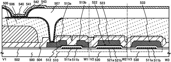
1. A semiconductor device comprising:
a transistor;
a capacitor electrically connected to the transistor; and
a light-emitting element electrically connected to the transistor,
wherein the transistor comprises:
a first conductive layer functioning as a gate electrode layer over a substrate;
a first insulating film over the first conductive layer;
a first oxide semiconductor film comprising a channel formation region;
a second conductive layer functioning as one of a source electrode and a drain electrode; and
a third conductive layer functioning as the other of the source electrode and the drain electrode,
wherein the capacitor comprises a second oxide semiconductor film,
wherein the semiconductor device further comprises:
a fourth conductive layer comprising a region in contact with a top surface of the second oxide semiconductor film;
a fifth conductive layer comprising a region intersecting with the first conductive layer when seen from above;
a second insulating film over the second conductive layer, the third conductive layer, and the fourth conductive layer; and
an electrode over and in contact with the second conductive layer through an opening of the second insulating film, the electrode functioning as a pixel electrode of the light-emitting element, and
wherein the second conductive layer, the third conductive layer, the fourth conductive layer, and the fifth conductive layer comprises the same material, and
wherein a concentration of one of chlorine and fluorine on a top surface of the gate electrode layer is 5×10¹⁸ atoms/cm3 or lower.
|