| CPC H01L 29/785 (2013.01) [H01L 25/074 (2013.01); H01L 29/0847 (2013.01); H01L 29/7827 (2013.01)] | 12 Claims |
|
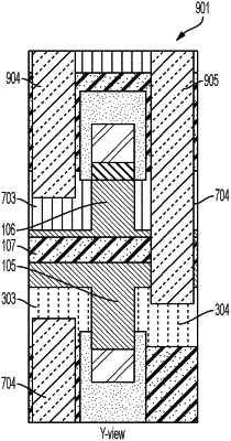
1. A semiconductor device fabrication method comprising:
frontside semiconductor device processing on a frontside of a wafer to form a frontside gate structure;
flipping the wafer;
backside semiconductor device processing on a backside of the wafer to form a backside gate structure, which is aligned with the frontside gate structure;
backside contact formation processing on the backside of the wafer following the frontside and backside semiconductor processing; and
frontside contact formation processing on the frontside of the wafer following the backside contact formation processing,
wherein the backside and frontside contact formation processing comprises at least one of:
forming an extended contact that extends in a normal direction from the backside of the wafer, through a backside dielectric layer and backside source/drain (S/D) regions of the backside of the wafer so as to be completely surrounded by the backside dielectric layer and the backside S/D regions and to the frontside of the wafer with straight sides extending through the backside dielectric layer and the backside S/D regions in the normal direction; and
forming an extended contact that extends in the normal direction from the frontside of the wafer, through a frontside dielectric layer and frontside S/D regions of the frontside of the wafer so as to be completely surrounded by the frontside dielectric layer and the frontside S/D regions and to the backside of the wafer with straight, opposite sides extending through the frontside dielectric layer and the frontside S/D regions in the normal direction.
|