| CPC H01L 29/7848 (2013.01) [H01L 21/02521 (2013.01); H01L 21/28518 (2013.01); H01L 21/823814 (2013.01); H01L 21/823821 (2013.01); H01L 21/823871 (2013.01); H01L 21/823878 (2013.01); H01L 27/0924 (2013.01); H01L 29/0653 (2013.01); H01L 29/0847 (2013.01); H01L 29/24 (2013.01); H01L 29/267 (2013.01); H01L 29/66492 (2013.01); H01L 29/66545 (2013.01); H01L 29/66636 (2013.01); H01L 29/66795 (2013.01); H01L 29/7833 (2013.01); H01L 29/7851 (2013.01)] | 20 Claims |
|
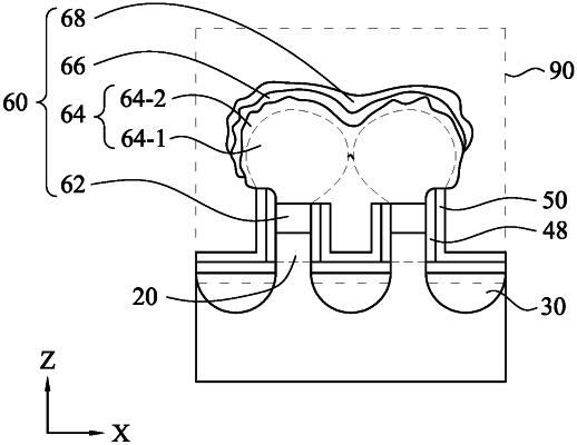
1. A semiconductor device comprising:
an isolation insulating layer disposed over a substrate;
a first fin structure disposed over the substrate;
a gate structure disposed over a channel region of the first fin structure;
a first source/drain epitaxial layer disposed over the first fin structure; and
a first fin liner layer disposed on side faces of a part of the first in structure and a part of the first epitaxial layer, wherein:
the first fin liner layer includes a lower portion disposed on one of the side faces and a higher portion disposed on another of the side faces,
a height of the lower portion is smaller than a height of the higher portion, and
the first fin liner layer includes a vertical portion having a first dielectric layer and a second dielectric layer and a horizontal portion having the second dielectric layer and not having the first dielectric layer.
|