| CPC H01L 29/737 (2013.01) [H01L 24/13 (2013.01); H01L 29/66242 (2013.01); H01L 29/66318 (2013.01); H01L 2224/0401 (2013.01)] | 20 Claims |
|
1. A semiconductor device comprising:
a substrate;
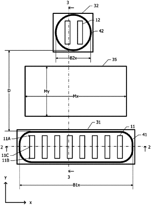
a plurality of first transistors each including a mesa structure configured of a semiconductor arranged on an upper surface, which is one surface of the substrate;
a first bump which is arranged at a position overlapping the plurality of first transistors in plan view, has a shape elongated in one direction in plan view, and is connected to the plurality of first transistors;
a second bump which is arranged so as to have a space with respect to the first bump in a direction orthogonal to a longitudinal direction of the first bump; and
a first metal pattern which is arranged between the first bump and the second bump in plan view, wherein
when the upper surface of the substrate is taken as a height reference, a center of the first metal pattern in a thickness direction has a height higher than an upper surface of the mesa structure included in each of the plurality of first transistors and lower than a lower surface of the first bump.
|