US 11,817,484 B2
Method for manufacturing an electronic device
Franck Julien, La Penne sur Huveaune (FR); Stephan Niel, Meylan (FR); and Leo Gave, Montpellier (FR)
Assigned to STMICROELECTRONICS (CROLLES 2) SAS, Crolles (FR); and STMICROELECTRONICS (ROUSSET) SAS, Rousset (FR)
Filed by STMICROELECTRONICS (CROLLES 2) SAS, Crolles (FR); and STMICROELECTRONICS (ROUSSET) SAS, Rousset (FR)
Filed on Sep. 27, 2022, as Appl. No. 17/935,754.
Application 17/935,754 is a continuation of application No. 17/100,559, filed on Nov. 20, 2020, granted, now 11,522,057.
Claims priority of application No. 1913092 (FR), filed on Nov. 22, 2019.
Prior Publication US 2023/0012522 A1, Jan. 19, 2023
This patent is subject to a terminal disclaimer.
Int. Cl. H01L 29/40 (2006.01); H01L 29/51 (2006.01); H01L 29/66 (2006.01)
CPC H01L 29/401 (2013.01) [H01L 29/518 (2013.01); H01L 29/6634 (2013.01)] 14 Claims
OG exemplary drawing
 
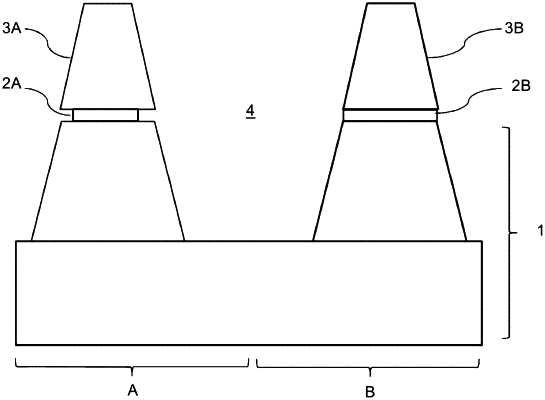
1. A device, comprising:
a substrate having a first surface, the substrate including:
a first extension of the substrate that extends away from the first surface, sidewalls of the first extension are tapered, the first extension having a second surface;
a first portion of an insulating layer on the second surface of the first extension, wherein the first portion of the insulating layer includes an undercut;
a first portion of a silicon nitride layer on the first portion of the insulating layer, sidewalls of the first portion of the silicon nitride layer are tapered.