| CPC H01L 29/0653 (2013.01) [H01L 21/763 (2013.01); H01L 21/76224 (2013.01); H01L 29/0847 (2013.01)] | 20 Claims |
|
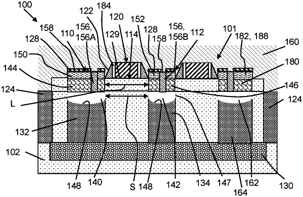
1. A transistor, comprising:
a bulk semiconductor substrate;
a first raised source/drain region above the bulk semiconductor substrate separated from a second raised source/drain region above the bulk semiconductor substrate;
a gate between the first raised source/drain region and the second raised source/drain region;
a first dielectric section beneath the first raised source/drain region in the bulk semiconductor substrate;
a second dielectric section beneath the second raised source/drain region in the bulk semiconductor substrate;
a first air gap defined in at least the first dielectric section and under the first raised source/drain region;
a second air gap defined in at least the second dielectric section and under the second raised source/drain region; and
a first filled vent hole extending through the first raised source/drain region and a second filled vent hole extending through the second raised source/drain region.
|