| CPC H01L 29/0623 (2013.01) [H01L 29/1608 (2013.01)] | 20 Claims |

|
1. A semiconductor device:
a substrate of a first conductivity type;
an active region disposed in the substrate, the active region including at least one active device; and
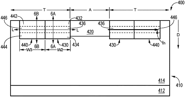
a termination region disposed in the substrate adjacent to the active region, the termination region excluding an active device, the termination region including a junction termination extension (JTE) of a second conductivity type, the second conductivity type being opposite the first conductivity type, the JTE having:
a first depletion stopper region disposed in an upper portion of the JTE;
a second depletion stopper region disposed in a lower portion of the JTE; and
a high carrier mobility region disposed between the first depletion stopper region and the second depletion stopper region, the high carrier mobility region having a constant doping region extending over a range of depths of the high carrier mobility region in the substrate, the high carrier mobility region having a carrier mobility that is greater than respective carrier mobilities of the first depletion stopper region and the second depletion stopper region.
|
|
15. A semiconductor device:
a substrate of a first conductivity type;
an active region disposed in the substrate, the active region including at least one active device; and
a termination region disposed in the substrate adjacent to the active region, the termination region excluding an active device, the termination region including a junction termination extension (JTE) of a second conductivity type, the second conductivity type being opposite the first conductivity type, the JTE having:
a first depletion stopper region extending from a surface of the substrate to a first depth in the substrate;
a high carrier mobility region extending from the first depth in the substrate to a second depth in the substrate, the second depth being greater than the first depth, the high carrier mobility region having a constant doping region extending over a range of depths between the first depth and the second depth; and
a second depletion stopper region extending from the second depth in the substrate to a third depth in the substrate, the third depth being greater than the second depth,
the high carrier mobility region having a carrier mobility that is greater than respective carrier mobilities of the first depletion stopper region and the second depletion stopper region.
|
|
18. A semiconductor device:
a substrate including:
a heavily-doped n-type silicon carbide substrate; and
a lightly-doped n-type silicon carbide epitaxial layer disposed on the heavily-doped n-type silicon carbide substrate;
an active region disposed in the lightly-doped n-type silicon carbide epitaxial layer, the active region including at least one of:
a power diode; or
a power n-channel metal-oxide semiconductor field-effect transistor (MOSFET); and
a termination region disposed in the lightly-doped n-type silicon carbide epitaxial layer adjacent to the active region, the termination region excluding an active device, the termination region including a p-type junction termination extension (JTE), the p-type JTE having:
a first depletion stopper region extending from a surface of the substrate to a first depth in the substrate;
a high carrier mobility region extending from the first depth in the substrate to a second depth in the substrate, the second depth being greater than the first depth, the high carrier mobility region having a constant doping region extending over a range of depths between the first depth and the second depth; and
a second depletion stopper region extending from the second depth in the substrate to a third depth in the substrate, the third depth being greater than the second depth,
the high carrier mobility region having a carrier mobility that is greater than respective carrier mobilities of the first depletion stopper region and the second depletion stopper region.
|