| CPC H01L 27/156 (2013.01) [H01L 33/38 (2013.01); H01L 33/62 (2013.01)] | 20 Claims |
|
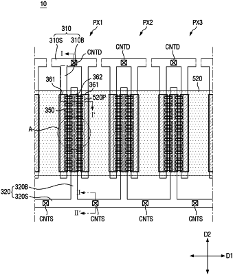
1. A display device, comprising:
a first electrode on a substrate;
a second electrode spaced apart from the first electrode on the substrate;
a first insulating layer disposed on the first electrode and the second electrode;
a second insulating layer disposed on the first insulating layer, and defining openings overlapping with at a least a portion of the first electrode and the second electrode, and with an area between the first electrode and the second electrode; and
a plurality of light emitting elements disposed in the openings and on the first electrode and the second electrode,
wherein the openings of the second insulating layer expose the first insulating layer, and
wherein the second insulating layer comprises a bridge portion between the openings.
|