US 11,817,473 B2
Solid-state imaging device, drive method thereof and electronic apparatus
Taiichiro Watanabe, Kanagawa (JP); Akihiro Yamada, Kanagawa (JP); Hideo Kido, Kanagawa (JP); Hiromasa Saito, Kanagawa (JP); Keiji Mabuchi, Kanagawa (JP); and Yuko Ohgishi, Tokyo (JP)
Assigned to SONY GROUP CORPORATION, Tokyo (JP)
Filed by Sony Group Corporation, Tokyo (JP)
Filed on Sep. 2, 2022, as Appl. No. 17/902,664.
Application 14/082,832 is a division of application No. 12/480,351, filed on Jun. 8, 2009, granted, now 8,614,759, issued on Dec. 24, 2013.
Application 17/902,664 is a continuation of application No. 16/932,544, filed on Jul. 17, 2020, granted, now 11,489,001.
Application 16/932,544 is a continuation of application No. 16/228,244, filed on Dec. 20, 2018, granted, now 10,748,958, issued on Aug. 18, 2020.
Application 16/228,244 is a continuation of application No. 14/082,832, filed on Nov. 18, 2013, granted, now 10,199,427, issued on Feb. 5, 2019.
Claims priority of application No. 2008-150963 (JP), filed on Jun. 9, 2008; application No. 2008-285907 (JP), filed on Oct. 6, 2008; application No. 2008-285908 (JP), filed on Nov. 6, 2008; and application No. 2008-285909 (JP), filed on Nov. 6, 2008.
Prior Publication US 2022/0415961 A1, Dec. 29, 2022
This patent is subject to a terminal disclaimer.
Int. Cl. H01L 27/148 (2006.01); H01L 27/146 (2006.01)
CPC H01L 27/14887 (2013.01) [H01L 27/1464 (2013.01); H01L 27/14603 (2013.01); H01L 27/14641 (2013.01); H01L 27/14647 (2013.01); H01L 27/14625 (2013.01); H01L 27/14656 (2013.01)] 20 Claims
OG exemplary drawing
 
1. A light detecting device, comprising:
a photoelectric converter;
a transfer transistor electrically connected to the photoelectric converter; and
a floating diffusion electrically connected to the transfer transistor,
wherein the transfer transistor is disposed on a first surface of a substrate which is opposite to a second surface of the substrate, the second surface being a light incident surface of the substrate,
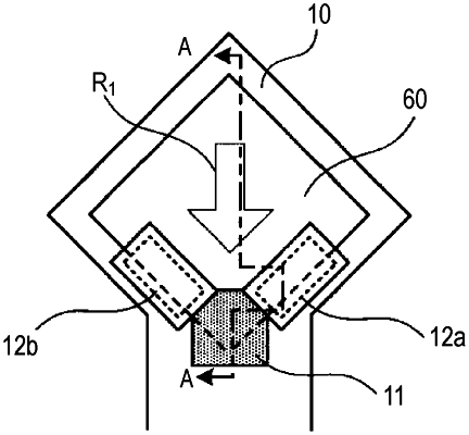
wherein the transfer transistor comprises a planar gate electrode disposed on the first surface of the substrate and first and second vertical gate electrodes disposed in the substrate, and
wherein the floating diffusion overlaps the photoelectric converter in a plan view.