| CPC H01L 27/14634 (2013.01) [H01L 27/14636 (2013.01)] | 20 Claims |
|
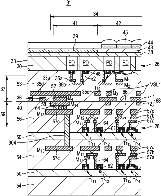
1. An imaging device, comprising:
a first chip including:
a first semiconductor substrate including a photoelectric conversion region that converts incident light into an electric charge; and
a first insulating layer including a first multilayer wiring electrically connected to the photoelectric conversion region, wherein the first multilayer wiring includes a first vertical signal line (VSL1) to output a first pixel signal based on the electric charge; and
a second chip including:
a second semiconductor substrate including a plurality of transistors;
a third semiconductor substrate; and
a second insulating layer including a second multilayer wiring electrically connected to the plurality of transistors, wherein the second multilayer wiring includes a first wiring that is connected to a second wiring in the third semiconductor substrate through a conductive via, and wherein the first wiring, the second wiring and the conductive via are located in a peripheral portion of the first chip.
|