| CPC H01L 27/14618 (2013.01) [H01L 23/13 (2013.01); H01L 24/32 (2013.01); H01L 24/73 (2013.01); H01L 27/14636 (2013.01); H01L 2224/32057 (2013.01); H01L 2224/32237 (2013.01); H01L 2224/73204 (2013.01)] | 5 Claims |
|
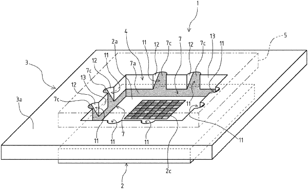
1. A solid-state imaging device comprising:
a solid-state imaging element having a pixel region which is a light receiving region including a large number of pixels on a surface side which is one plate surface of a semiconductor substrate;
a substrate provided on the surface side with respect to the solid-state imaging element and having an opening for passing light to be received by the pixel region; and
an underfill part formed including a cured fluid and covering a connection part that electrically connects the solid-state imaging element and the substrate,
wherein the substrate has a groove for guiding the fluid forming the underfill part in a direction away from the surface of the solid-state imaging element, on a surface portion forming the opening.
|