| US 11,817,465 B2 | ||
| Image sensors | ||
| Jung Bin Yun, Hwaseong (KR); Eun Sub Shim, Hwaseong (KR); Kyung Ho Lee, Suwon (KR); Sung Ho Choi, Seoul (KR); Jung Hoon Park, Hwaseong (KR); Jung Wook Lim, Gunpo (KR); and Min Ji Jung, Daegu (KR) | ||
| Assigned to Samsung Electronics Co., Ltd., Suwon-si (KR) | ||
| Filed by Samsung Electronics Co., Ltd., Suwon-si (KR) | ||
| Filed on Jan. 18, 2023, as Appl. No. 18/155,785. | ||
| Application 18/155,785 is a continuation of application No. 17/399,282, filed on Aug. 11, 2021, granted, now 11,581,344, issued on Feb. 14, 2023. | ||
| Application 17/399,282 is a continuation of application No. 16/711,987, filed on Dec. 12, 2019, granted, now 11,121,157, issued on Sep. 14, 2021. | ||
| Application 16/711,987 is a continuation of application No. 15/862,013, filed on Jan. 4, 2018, granted, now 10,573,676, issued on Feb. 25, 2020. | ||
| Claims priority of application No. 10-2017-0045155 (KR), filed on Apr. 7, 2017. | ||
| Prior Publication US 2023/0154946 A1, May 18, 2023 | ||
| Int. Cl. H01L 27/146 (2006.01); H04N 25/70 (2023.01); H04N 25/778 (2023.01) | ||
| CPC H01L 27/14605 (2013.01) [H01L 27/14627 (2013.01); H01L 27/14641 (2013.01); H04N 25/70 (2023.01); H04N 25/778 (2023.01)] | 18 Claims |
|
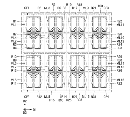
1. An image sensor comprising:
a first pixel group comprising a 1st photoelectric conversion element to an 8th photoelectric conversion element and a 1st microlens to a 4th microlens; a second pixel group comprising a 9th photoelectric conversion element to a 16th photoelectric conversion element and a 5th microlens to an 8th microlens; a third pixel group comprising a 17th photoelectric conversion element to a 24th photoelectric conversion element and a 9th microlens to a 12th microlens; and a fourth pixel group comprising a 25th photoelectric conversion element to a 32nd photoelectric conversion element and a 13th microlens to a 16th microlens; wherein the second pixel group is disposed adjacent to the first pixel group in a first direction, wherein the third pixel group is disposed adjacent to the first pixel group in a second direction perpendicular to the first direction, wherein the fourth pixel group is disposed adjacent to the second pixel group in the second direction and is disposed adjacent to the third pixel group in the first direction, wherein each of the nth microlens is disposed to overlap at least a portion of the (2xn∼1)th photoelectric conversion elements and at least a portion of the (2xn)thphotoelectric conversion elements in a plan view and is spaced apart from the (2xn-1)th photoelectric conversion elements and the (2xn)th photoelectric conversion elements in a third direction perpendicular to the first direction and the second direction, n is integer in a range of 1 to 16, wherein a first color filter is disposed between the 1st photoelectric conversion element to the 8th photoelectric conversion element and the 1st microlens to the 4th microlens, wherein a second color filter is disposed between the 9th photoelectric conversion element to the 16th photoelectric conversion element and the 5th microlens to the 8th microlens, wherein a third color filter is disposed between the 17th photoelectric conversion element to the 24th photoelectric conversion element and the 9th microlens to the 12th microlens, and wherein a fourth color filter is disposed between the 25th photoelectric conversion element to the 32nd photoelectric conversion element and the 13th microlens to the 16th microlens. |