| CPC H01L 27/1225 (2013.01) [G02F 1/1368 (2013.01); H01L 27/127 (2013.01); H01L 27/1462 (2013.01); H01L 27/14616 (2013.01); H01L 27/14685 (2013.01); H01L 27/14692 (2013.01); G02F 1/134363 (2013.01); H01L 27/14658 (2013.01)] | 20 Claims |

|
1. An active matrix substrate comprising:
a substrate; and
at least one thin film transistor supported by the substrate,
wherein each thin film transistor includes an oxide semiconductor layer, a gate electrode disposed closer to the substrate side of the oxide semiconductor layer, a gate insulating layer disposed between the oxide semiconductor layer and the gate electrode, a source electrode, and a drain electrode,
the oxide semiconductor layer includes a layered structure including
a first layer and
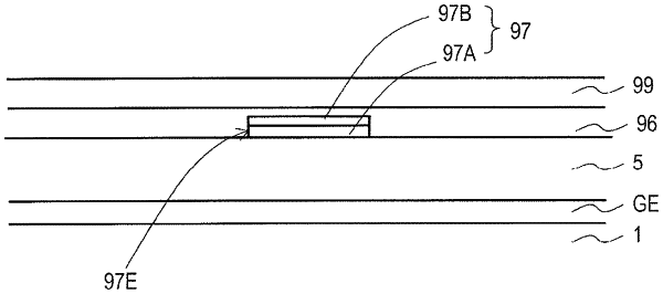
a second layer disposed on a part of the first layer and extending across the first layer in a channel width direction when viewed in a normal direction of the substrate,
the first layer includes an overlapping portion overlapping with the second layer, and a first portion and a second portion each located on a corresponding one of both sides of the second layer, when viewed in a normal direction of the substrate,
the second layer covers an upper surface and a side surface of the overlapping portion of the first layer,
the source electrode is electrically connected to at least a part of an upper surface of the first portion,
the drain electrode is electrically connected to at least a part of an upper surface of the second portion,
an etch stop layer is located between the oxide semiconductor layer and the source electrode and between the oxide semiconductor layer and the drain electrode and covers at least a part of the oxide semiconductor layer,
the etch stop layer includes a first opening exposing at least the part of the first portion of the first layer and a second opening exposing at least the part of the second portion of the first layer,
the source electrode is connected to the first portion in the first opening, and
the drain electrode is connected to the second portion in the second opening.
|