US 11,817,458 B2
Display device
Ki Hyun Kim, Hwaseong-si (KR); Young Gil Park, Anyang-si (KR); Jin Suk Lee, Gwangmyeong-si (KR); Jai Sun Kyoung, Cheonan-si (KR); and Sug Woo Jung, Hwaseong-si (KR)
Assigned to Samsung Display Co., Ltd., Yongin-si (KR)
Filed by Samsung Display Co., Ltd., Yongin-si (KR)
Filed on Jul. 21, 2020, as Appl. No. 16/935,063.
Claims priority of application No. 10-2019-0159525 (KR), filed on Dec. 4, 2019.
Prior Publication US 2021/0175258 A1, Jun. 10, 2021
Int. Cl. H01L 27/12 (2006.01); H10K 59/121 (2023.01)
CPC H01L 27/1218 (2013.01) [H01L 27/1225 (2013.01); H01L 27/1248 (2013.01)] 20 Claims
OG exemplary drawing
 
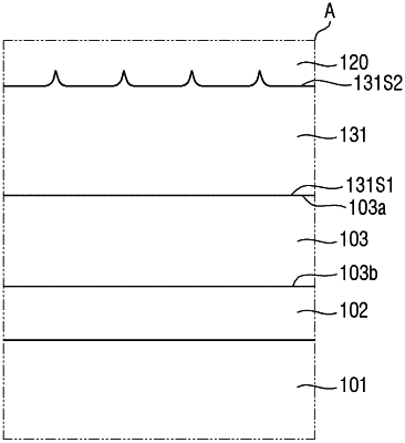
1. A display device, comprising:
a substrate;
a polycrystalline silicon film on the substrate; and
a first buffer film between the substrate and the polycrystalline silicon film and having one surface contacting the polycrystalline silicon film and another surface opposite to the one surface,
wherein the one surface of the first buffer film has a first root mean square (RMS) roughness range, and the first RMS roughness range is 1.5 nm or less.