US 11,817,454 B2
Polysilicon resistor using reduced grain size polysilicon
Yanbiao Pan, Plano, TX (US); Robert Martin Higgins, Plano, TX (US); Bhaskar Srinivasan, Allen, TX (US); and Pushpa Mahalingam, Richardson, TX (US)
Assigned to Texas Instruments Incorporated, Dallas, TX (US)
Filed by Yanbiao Pan, Plano, TX (US); Robert Martin Higgins, Plano, TX (US); Bhaskar Srinivasan, Allen, TX (US); and Pushpa Mahalingam, Richardson, TX (US)
Filed on Aug. 31, 2021, as Appl. No. 17/463,252.
Claims priority of provisional application 63/141,144, filed on Jan. 25, 2021.
Prior Publication US 2022/0238516 A1, Jul. 28, 2022
Int. Cl. H01L 27/08 (2006.01); H01L 21/02 (2006.01); H01L 49/02 (2006.01)
CPC H01L 27/0802 (2013.01) [H01L 21/02595 (2013.01); H01L 28/20 (2013.01)] 20 Claims
OG exemplary drawing
 
1. A resistor comprising:
a non-conductive surface over a semiconductor substrate;
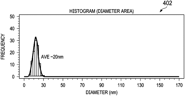
a patterned polysilicon layer on the non-conductive surface, the patterned polysilicon layer including polycrystalline silicon wherein 50% of grains in the polycrystalline silicon have a diameter smaller than 20 nm;
a first terminal connected to the patterned polysilicon layer; and
a second terminal connected to the patterned polysilicon layer and spaced apart from the first terminal.