| CPC H01L 27/0629 (2013.01) [H01G 11/14 (2013.01); H01L 27/1207 (2013.01); H01L 27/1211 (2013.01); H01L 27/1225 (2013.01); H01L 29/66742 (2013.01); H01L 29/786 (2013.01); H01L 29/7869 (2013.01); H01L 29/78696 (2013.01); H01G 11/08 (2013.01); H01L 21/8258 (2013.01); H01L 27/0688 (2013.01); Y02E 60/13 (2013.01)] | 3 Claims |
|
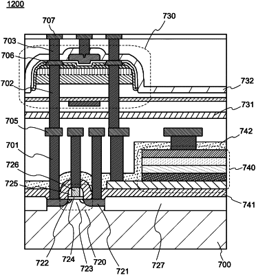
1. A semiconductor device comprising:
a first circuit comprising a first transistor;
a first insulating film over the first transistor;
a capacitor over the first insulating film;
a second insulating film over the capacitor; and
a second circuit comprising a second transistor over the second insulating film,
wherein the second transistor comprises a semiconductor comprising a channel formation region,
wherein the semiconductor comprises a first opening and a second opening,
wherein a first connection electrode penetrates the semiconductor through the first opening,
wherein a second connection electrode penetrates the semiconductor through the second opening, and
wherein the first circuit and the second circuit are electrically connected by the first connection electrode.
|