| CPC H01L 27/0277 (2013.01) [H01L 27/0274 (2013.01); H01L 27/0285 (2013.01)] | 20 Claims |
|
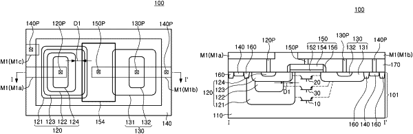
1. A semiconductor device comprising:
a substrate;
a separation region in the substrate;
an electrostatic discharge protection element;
an internal integrated circuit electrically connected to the electrostatic discharge protection element; and
a first pad and a second pad electrically connected to the electrostatic discharge protection element and the internal integrated circuit,
wherein the electrostatic discharge protection element comprises:
a P-well region in the substrate;
a gate structure including a gate electrode having a first side surface and a second side surface, opposing each other, on the substrate, a gate spacer, and a gate dielectric layer between the gate electrode and the substrate;
a first region adjacent to the first side surface of the gate electrode in the substrate;
a second region adjacent to the second side surface of the gate electrode in the substrate; and
a first contact plug electrically connected to the first region, and wherein
the first region and the second region have N-type conductivity,
the first region includes a first N-well region in the substrate, a second N-well region in the first N-well region, a first impurity region overlapping the second N-well region in the first N-well region in a vertical direction, and a second impurity region nested in the first impurity region, the second impurity region having a smaller width than the first impurity region, the first impurity region having a top surface extending flat from an edge of the second impurity region to an outer edge of the first impurity region, the top surfaces of the first and second impurity regions being coplanar,
the first N-well region, the second N-well region, the first impurity region, and the second impurity region have different doping concentrations,
the second region includes a third impurity region in the substrate and a fourth impurity region in the third impurity region,
the vertical direction is perpendicular to an upper surface of the substrate,
a distance between the upper surface of the substrate and a lower surface of the second N-well region is greater than a distance between the upper surface of the substrate and a lower surface of the separation region,
the first contact plug is in contact with the second impurity region in the first region, and
the gate electrode overlaps the first impurity region and not the second impurity region when viewed from above.
|