| CPC H01L 25/50 (2013.01) [H01L 21/563 (2013.01); H01L 23/5381 (2013.01); H01L 23/5385 (2013.01); H01L 24/06 (2013.01); H01L 24/11 (2013.01); H01L 24/16 (2013.01); H01L 24/17 (2013.01); H01L 25/18 (2013.01); H01L 2224/0603 (2013.01); H01L 2224/11013 (2013.01); H01L 2224/16145 (2013.01); H01L 2224/16227 (2013.01); H01L 2224/16238 (2013.01); H01L 2224/1703 (2013.01); H01L 2224/17051 (2013.01)] | 20 Claims |
|
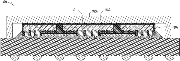
1. A multi-chip package, comprising:
a bridge interconnect in a molding material, the bridge interconnect comprising a first plurality of bridge contacts and a second plurality of bridge contacts, and the bridge interconnect having a bottommost surface;
a first plurality of die vias in the molding material, the first plurality of die vias laterally adjacent to a first side of the bridge interconnect, and the first plurality of die vias having a bottommost surface co-planar with the bottommost surface of the bridge interconnect;
a second plurality of die vias in the molding material, the second plurality of die vias laterally adjacent to a second side of the bridge interconnect, the second side opposite the first side, and the second plurality of die vias having a bottommost surface co-planar with the bottommost surface of the bridge interconnect;
a first die electrically coupled to the first plurality of bridge contacts of the bridge interconnect, and the first die electrically coupled to the first plurality of die vias;
a second die electrically coupled to the second plurality of bridge contacts of the bridge interconnect, and the second die electrically coupled to the second plurality of die vias
a first plurality of solder balls vertically beneath the bridge interconnect; and
a second plurality of solder balls vertically beneath the first plurality of die vias and vertically beneath the first die, wherein individual ones of the second plurality of solder balls are larger than individual ones of the first plurality of solder balls.
|