| CPC H01L 25/18 (2013.01) [H01L 23/481 (2013.01); H01L 23/5384 (2013.01); H01L 24/05 (2013.01); H01L 24/14 (2013.01)] | 17 Claims |
|
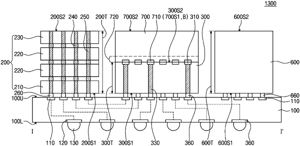
1. A semiconductor package, comprising:
a substrate;
a first semiconductor chip on the substrate;
the first semiconductor chip including a plurality of first chip pads adjacent to a top surface of the first semiconductor chip;
a second semiconductor chip on the substrate, the second semiconductor chip laterally spaced apart from the first semiconductor chip; and
an upper semiconductor chip on the first semiconductor chip,
a bottom surface of the upper semiconductor chip facing the top surface of the first semiconductor chip,
the upper semiconductor chip including a plurality of second chip pads adjacent to the bottom surface of the upper semiconductor chip,
the plurality of second chip pads being directly connected to the plurality of first chip pads, and
the second semiconductor chip arranged so the top surface of the first semiconductor chip is lower than a top surface of the second semiconductor chip, wherein
the first semiconductor chip includes a plurality of through electrodes that penetrate an inside of the first semiconductor chip, and
the plurality of through electrodes are connected to corresponding ones of the plurality of second chip pads through corresponding ones of the plurality of first chip pads, wherein
the second semiconductor chip includes a plurality of sub-semiconductor chips that are stacked in a direction perpendicular to a top surface of the substrate, and
the plurality of sub-semiconductor chips include a plurality of memory chips.
|