| CPC H01L 25/167 (2013.01) [G09G 3/32 (2013.01); H10K 59/1213 (2023.02); G09G 2300/0426 (2013.01); G09G 2300/0842 (2013.01); G09G 2320/0242 (2013.01); G09G 2320/043 (2013.01); G09G 2330/021 (2013.01); H01L 27/124 (2013.01); H10K 59/353 (2023.02)] | 20 Claims |
|
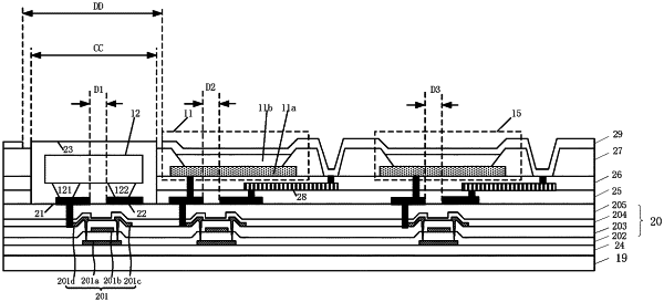
1. A display panel, comprising:
a plurality of pixels, wherein:
a pixel of the plurality of pixels includes a light-emitting layer,
the plurality of pixels include at least one first pixel and at least one second pixel,
a first pixel of the at least one first pixel is electrically connected to a first pixel circuit, and a second pixel of the at least one second pixel is electrically connected to a second pixel circuit,
an orthographic projection of the first pixel circuit on a plane of the display panel has an area smaller than an orthographic projection of the second pixel circuit on the plane of the display panel, and
in a direction perpendicular to the plane of the display panel, a light-emitting layer of the first pixel at least partially overlaps the second pixel circuit, and a light-emitting layer of the second pixel at least partially overlaps the second pixel circuit,
wherein the display panel further comprises:
a substrate,
an array layer, disposed on a side of substrate, wherein the first pixel and the second pixel are disposed on a side of the array layer away from the substrate, and
an encapsulation structure, disposed on the side of the array layer away from the substrate, wherein the encapsulation structure is configured to encapsulate the second pixel.
|