| CPC H01L 25/167 (2013.01) [H01L 21/6835 (2013.01); H01L 24/19 (2013.01); H01L 24/97 (2013.01); H01L 25/0753 (2013.01); H01L 27/1214 (2013.01); H01L 33/0093 (2020.05); H01L 33/06 (2013.01); H01L 33/325 (2013.01); H01L 33/38 (2013.01); H01L 33/502 (2013.01); H01L 33/58 (2013.01); H01L 33/62 (2013.01); H05B 33/12 (2013.01); H05B 33/14 (2013.01); G09G 3/32 (2013.01); G09G 2300/04 (2013.01); G09G 2300/0452 (2013.01); G09G 2300/08 (2013.01); H01L 27/156 (2013.01); H01L 33/0095 (2013.01); H01L 33/42 (2013.01); H01L 33/504 (2013.01); H01L 33/507 (2013.01); H01L 2221/68322 (2013.01); H01L 2221/68327 (2013.01); H01L 2221/68336 (2013.01); H01L 2221/68354 (2013.01); H01L 2221/68368 (2013.01); H01L 2224/45099 (2013.01); H01L 2224/4911 (2013.01); H01L 2924/00 (2013.01); H01L 2924/00014 (2013.01); H01L 2924/12041 (2013.01); H01L 2933/0066 (2013.01)] | 20 Claims |
|
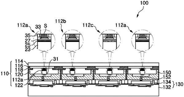
1. A display apparatus comprising:
a support substrate;
a plurality of light emitting structures regularly arranged on the support substrate; and
a wavelength conversion part disposed on the plurality of light emitting structures,
wherein the wavelength conversion part includes light transmitting regions and blocking regions, the light transmitting regions disposed on the light emitting structures, respectively, and each of the light transmitting regions includes a wavelength converter for converting a wavelength of light emitted from the corresponding light emitting structure, and
wherein the support substrate comprises a plurality of conductive patterns electrically connected to the light emitting structures, and the light emitting structures are coupled to the plurality of conductive patterns.
|