| CPC H01L 25/0756 (2013.01) [H01L 24/32 (2013.01); H01L 24/33 (2013.01); H01L 25/0753 (2013.01); H01L 33/38 (2013.01); H01L 33/54 (2013.01); H01L 33/62 (2013.01); H01L 2224/32145 (2013.01); H01L 2224/33181 (2013.01); H01L 2924/12041 (2013.01)] | 17 Claims |
|
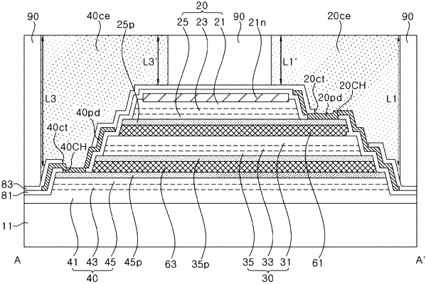
1. A light emitting device, comprising:
a first light emitting stack, a second light emitting stack, and a third light emitting stack, each including a first conductivity type semiconductor layer, a second conductivity type semiconductor layer, and an active layer disposed between the first and second conductivity type semiconductor layers;
a first lower contact electrode in ohmic contact with the first light emitting stack;
a second lower contact electrode in ohmic contact with the second conductivity type semiconductor layer of the second light emitting stack;
a third lower contact electrode in ohmic contact with the second conductivity type semiconductor layer of the third light emitting stack;
a first connection electrode electrically connected to the first light emitting stack;
a second connection electrode electrically connected to the second light emitting stack;
a third connection electrode electrically connected to the third light emitting stack; and
a fourth connection electrode commonly electrically connected to the first, second, and third light emitting stacks,
wherein:
the second light emitting stack is disposed between the first light emitting stack and the third light emitting stack;
the first lower contact electrode is disposed between the first light emitting stack and the second light emitting stack;
the second lower contact electrode and the third lower contact electrode are disposed between the second light emitting stack and the third light emitting stack;
the first lower contact electrode, the second lower contact electrode, and the third lower contact electrode include transparent conductive oxide layers;
a thickness of the second lower contact electrode or the third lower contact electrode is greater than a thickness of the first lower contact electrode;
the fourth connection electrode is electrically connected to the first conductivity type semiconductor layers of the first, second, and third light emitting stacks in common; and
the first conductivity type semiconductor layers comprise n-type semiconductor layers.
|