| CPC H01L 25/0657 (2013.01) [H01L 24/08 (2013.01); H01L 25/50 (2013.01); H10B 41/10 (2023.02); H10B 41/27 (2023.02); H10B 43/10 (2023.02); H10B 43/27 (2023.02); H10B 43/35 (2023.02); H10B 43/40 (2023.02); H10B 43/50 (2023.02); H01L 24/05 (2013.01); H01L 2224/0401 (2013.01); H01L 2224/05025 (2013.01); H01L 2224/05147 (2013.01); H01L 2224/05571 (2013.01); H01L 2224/08146 (2013.01); H01L 2225/06544 (2013.01); H01L 2225/06565 (2013.01)] | 8 Claims |
|
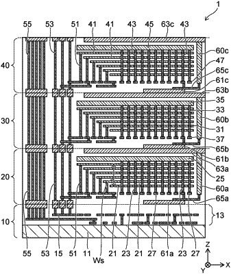
1. A memory device comprising:
a first memory cell array including a first stacked body, the first stacked body including a plurality of first electrode layers each extending in a first direction; and
a peripheral circuit facing the first memory cell array and driving the first memory cell array, the peripheral circuit and the first memory cell array being arranged in a second direction, the second direction crossing the first direction, the plurality of first electrode layers being stacked in the second direction, wherein
the plurality of first electrode layers each has a length along the first direction such that a first-first electrode layer of the plurality of first electric layers has a length shorter than a length of a second-first electrode layer of the plurality of first electric layers, and
the first-first electrode layer is positioned between the peripheral circuit and the second-first electrode layer.
|