| CPC H01L 25/0657 (2013.01) [H01L 23/5385 (2013.01); H01L 23/5386 (2013.01); H01L 24/14 (2013.01)] | 18 Claims |
|
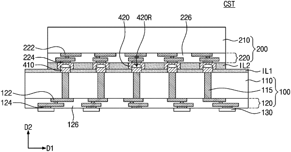
1. A semiconductor package, comprising:
a lower semiconductor chip having a first surface and a second surface, which are opposite to each other;
an upper semiconductor chip on the first surface of the lower semiconductor chip;
a first insulating layer between the first surface of the lower semiconductor chip and the upper semiconductor chip;
a second insulating layer between the first insulating layer and the upper semiconductor chip; and
a connection structure penetrating the first insulating layer and the second insulating layer and being connected to the lower semiconductor chip and the upper semiconductor chip,
wherein the connection structure comprises a first connecting portion and a second connecting portion, which are respectively disposed in the first insulating layer and the second insulating layer,
wherein a lower surface of the first connecting portion vertically overlaps the first surface of the lower semiconductor chip,
wherein the lower surface of the first connecting portion is in direct contact with the first surface of the lower semiconductor chip,
wherein a maximum width of the second connecting portion in a first direction is larger than a maximum width of the first connecting portion in the first direction,
wherein the first direction is parallel to the first surface of the lower semiconductor chip,
wherein the second connecting portion of the connection structure includes a connection pad with a recessed region,
wherein the first connection portion is inserted into the recessed region of the second connection portion,
wherein the first insulating layer is in direct contact with a bottom surface of the second connecting portion and a side surface of the first connecting portion, and
wherein a contact surface between the first insulating layer and the first connecting portion vertically overlaps the first surface of the lower semiconductor chip.
|