| CPC H01L 25/0652 (2013.01) [H01L 23/36 (2013.01); H01L 23/4334 (2013.01); H01L 23/49811 (2013.01); H01L 24/13 (2013.01); H01L 24/16 (2013.01); H01L 24/32 (2013.01); H01L 24/81 (2013.01); H01L 24/97 (2013.01); H01L 25/18 (2013.01); H01L 25/50 (2013.01); H01L 25/071 (2013.01); H01L 28/10 (2013.01); H01L 2224/16238 (2013.01); H01L 2225/06503 (2013.01); H01L 2225/06513 (2013.01); H01L 2225/06517 (2013.01); H01L 2225/06531 (2013.01); H01L 2225/06555 (2013.01); H01L 2225/06589 (2013.01)] | 6 Claims |
|
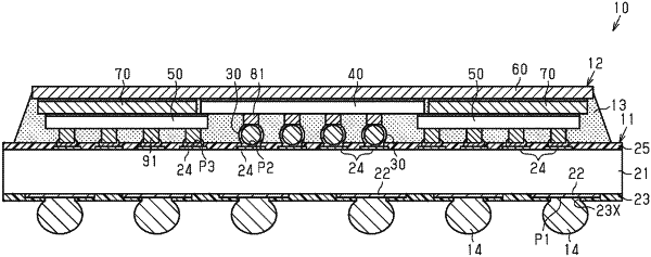
1. A semiconductor device, comprising:
a first semiconductor element;
a first connection terminal formed on a lower surface of the first semiconductor element;
a second semiconductor element mounted on the lower surface of the first semiconductor element so that the second semiconductor element partially overlaps the first semiconductor element in plan view;
a second connection terminal formed on a lower surface of the second semiconductor element;
a wiring substrate including a first connection pad electrically connected to the first connection terminal and a second connection pad electrically connected to the second connection terminal, wherein the first semiconductor element and the second semiconductor element are mounted over the wiring substrate;
a third connection terminal formed on the first connection pad and electrically connected to the first connection terminal;
a heat dissipation plate mounted on an upper surface of the first semiconductor element;
a spacer formed on a lower surface of the heat dissipation plate, wherein the second semiconductor element is mounted on a lower surface of the spacer; and
an underfill resin with which a gap between the heat dissipation plate and the wiring substrate is filled to encapsulate the first semiconductor element and the second semiconductor element, wherein
the first connection terminal is a metal post,
the third connection terminal is a core solder ball,
the core solder ball includes a spherical core ball and solder covering a periphery of the core ball,
the metal post is electrically connected to the core solder ball via a first solder layer,
a side surface of the spacer is separated from a side surface of the heat dissipation plate toward an inner side of the semiconductor device,
a side surface of the second semiconductor element is separated from the side surface of the spacer further toward the inner side of the semiconductor device,
the side surface and the lower surface of the heat dissipation plate, the side surface and the lower surface of the spacer, and the side surface and the lower surface of the second semiconductor element are formed in a stepped manner
the lower surface of the spacer is coplanar with the lower surface of the first semiconductor element, and
the second semiconductor element is bonded to the lower surface of the spacer and the lower surface of the first semiconductor element.
|