| CPC H01L 24/75 (2013.01) [B23K 1/0056 (2013.01); B23K 3/08 (2013.01); B23K 2101/40 (2018.08); H01L 2224/75261 (2013.01); H01L 2224/75745 (2013.01); H01L 2224/75984 (2013.01)] | 3 Claims |
|
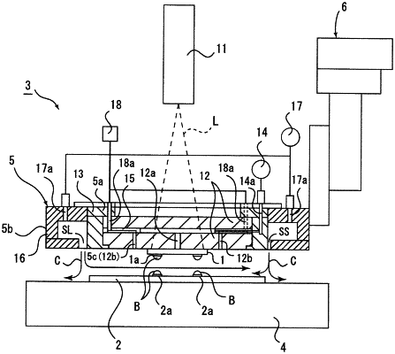
1. A bonding apparatus comprising:
a bonding stage that holds a substrate;
a bonding held provided with a holding section that holds a semiconductor chip;
a gas supplying unit;
a spray aperture provided adjacent to and surrounding the holding section of the bonding head, the gas supplying unit causing an inert gas to be sprayed from the spray aperture, a portion of the spray aperture being a large spray aperture and another portion of the spray aperture being a small spray aperture, the large spray aperture being set to a larger jet flow rate of the inert gas than the small spray aperture, the inert gas sprayed from the large spray aperture and the small spray aperture forming an air curtain that surrounds a bonding portion between the semiconductor chip and the substrate, the inert gas sprayed from the large spray aperture forming a flow that passes between the semiconductor chip and the substrate; and
a suction surface that holds the semiconductor chip by suction on the holding section of the bonding head, the holding section being formed into an approximately square shape with four edges, the spray aperture comprises four slits provided along the four edges of the holding section, respectively, and one or two of the slits form the large spray aperture.
|