| CPC H01L 24/29 (2013.01) [H01L 24/32 (2013.01); H01L 24/83 (2013.01); H01L 25/0753 (2013.01); H01L 33/60 (2013.01); H01L 33/62 (2013.01); H01L 2224/2929 (2013.01); H01L 2224/2957 (2013.01); H01L 2224/29339 (2013.01); H01L 2224/29344 (2013.01); H01L 2224/29347 (2013.01); H01L 2224/29355 (2013.01); H01L 2224/29371 (2013.01); H01L 2224/29411 (2013.01); H01L 2224/29439 (2013.01); H01L 2224/29455 (2013.01); H01L 2224/29499 (2013.01); H01L 2224/32227 (2013.01); H01L 2224/8302 (2013.01); H01L 2224/83091 (2013.01); H01L 2224/83099 (2013.01); H01L 2224/83192 (2013.01); H01L 2224/83851 (2013.01); H01L 2924/12041 (2013.01); H01L 2924/20105 (2013.01)] | 18 Claims |
|
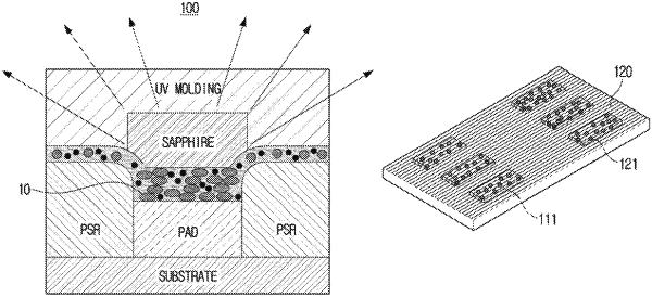
1. A display module, comprising:
a substrate;
a plurality of pads spaced from each other and disposed on the substrate;
a conduction film bonded to the plurality of pads disposed on the substrate, wherein at least one of a surface of the conduction film or an inner portion of the conduction film is black color treated; and
a display device mounted on the plurality of pads to which the conduction film is bonded,
wherein the conduction film is configured to electrically connect the display device to the plurality of pads disposed on the substrate,
wherein the conduction film comprises a plurality of conduction particles in a first portion of the conduction film where the plurality of pads are bonded to the conduction film,
wherein the first portion of the conduction film comprises conduction particles, among the plurality of conduction particles, that are adhered to one another to form an electrical connection between a corresponding pad of the plurality of pads and the display device, and
wherein the at least one of the surface of the conduction film or the inner portion of the conduction film that is black color treated is disposed between the plurality of pads and the display device.
|