| CPC H01L 24/16 (2013.01) [H01L 23/49816 (2013.01); H01L 23/49822 (2013.01); H01L 23/49833 (2013.01); H01L 23/49838 (2013.01); H01L 24/05 (2013.01); H01L 24/08 (2013.01); H01L 24/09 (2013.01); H01L 24/13 (2013.01); H01L 24/17 (2013.01); H01L 24/73 (2013.01); H01L 24/81 (2013.01); H01L 25/105 (2013.01); H01L 2224/05147 (2013.01); H01L 2224/05155 (2013.01); H01L 2224/0807 (2013.01); H01L 2224/0903 (2013.01); H01L 2224/13111 (2013.01); H01L 2224/16013 (2013.01); H01L 2224/16059 (2013.01); H01L 2224/16148 (2013.01); H01L 2224/1703 (2013.01); H01L 2224/73204 (2013.01); H01L 2224/81203 (2013.01); H01L 2924/1431 (2013.01); H01L 2924/1434 (2013.01)] | 20 Claims |

|
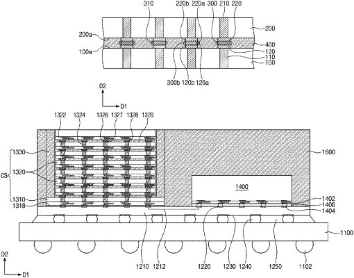
1. A semiconductor package, comprising:
a first die;
through electrodes penetrating the first die;
a first pad on a top surface of the first die and coupled to a through electrode from among the through electrodes;
a second die on the first die;
a second pad on a bottom surface of the second die;
a first connection terminal connecting the first pad to the second pad; and
an insulating layer filling a region between the first die and the second die and enclosing the first connection terminal,
wherein the first connection terminal comprises an intermetallic compound made of a solder material and metallic material of the first pad and the second pad, and
a concentration of the metallic material in the first connection terminal is substantially constant regardless of a distance from the first pad or the second pad.
|