| CPC H01L 24/05 (2013.01) [H01L 21/561 (2013.01); H01L 24/13 (2013.01); H01L 24/73 (2013.01); H01L 24/96 (2013.01); H01L 2224/0401 (2013.01); H01L 2224/12105 (2013.01); H01L 2224/13099 (2013.01); H01L 2224/81801 (2013.01); H01L 2924/1304 (2013.01); H01L 2924/18162 (2013.01)] | 20 Claims |
|
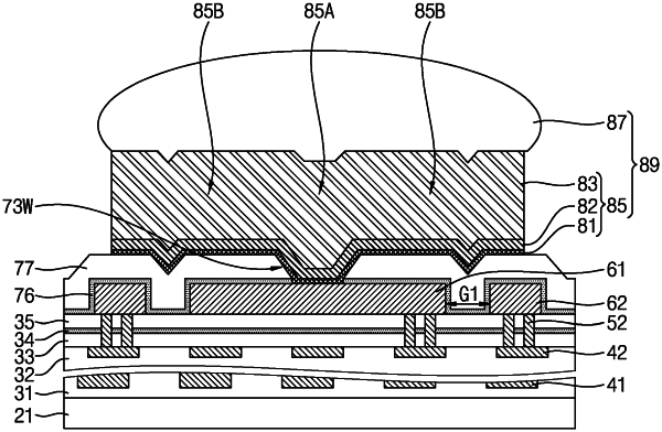
1. A semiconductor device comprising:
a substrate;
a lower insulating layer on the substrate;
a lower interconnection member in the lower insulating layer;
a pad on the lower insulating layer;
an upper interconnection member on the lower insulating layer;
a gap region between the pad and the upper interconnection member;
a protective insulating layer covering the lower insulating layer, the pad and the upper interconnection member; and
a bump arranged on the protective insulating layer and electrically connected to the pad,
wherein a thickness of the pad in a first direction that is perpendicular to a top surface of the substrate is greater than a thickness of the lower interconnection member in the first direction,
a width of the gap region in a second direction that is perpendicular to the first direction is greater than or equal to the thickness of the pad in the first direction,
the protective insulating layer includes an opening that is on the pad and a concave portion that is adjacent to the gap region, and
the bump includes a first convex portion in the opening of the protective insulating layer and a second convex portion in the concave portion of the protective insulating layer.
|