| CPC H01L 24/05 (2013.01) [H01L 24/03 (2013.01); H01L 24/11 (2013.01); H01L 24/13 (2013.01); H01L 24/16 (2013.01); H01L 25/0655 (2013.01); H01L 25/0657 (2013.01); H01L 2224/0231 (2013.01); H01L 2224/02331 (2013.01); H01L 2224/0401 (2013.01); H01L 2224/05082 (2013.01); H01L 2224/16146 (2013.01); H01L 2224/16227 (2013.01); H01L 2225/0652 (2013.01); H01L 2225/06517 (2013.01)] | 29 Claims |

|
1. An integrated circuit (IC) package, comprising:
a die, comprising:
a back end-of-line (BEOL) interconnect structure;
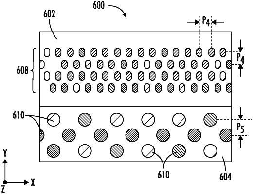
a plurality of under bump metallization (UBM) interconnects each coupled to the BEOL interconnect structure, the plurality of UBM interconnects comprising:
a first UBM interconnect; and
a second UBM interconnect that does not have a coupled interconnect bump; and
a raised interconnect bump coupled to the first UBM interconnect;
wherein the die further comprises:
a seed layer coupling the first UBM interconnect to the second UBM interconnect, to couple the raised interconnect bump to the second UBM interconnect;
wherein the BEOL interconnect structure comprises a metallization layer comprising:
a plurality of first metal interconnects comprising a plurality of metal pads, each of the plurality of first metal interconnects coupled to a UBM interconnect among the plurality of UBM interconnects; and
a second metal interconnect coupled to the second UBM interconnect.
|