| CPC H01L 24/02 (2013.01) [H01L 21/481 (2013.01); H01L 23/49822 (2013.01); H01L 23/49894 (2013.01); H01L 24/05 (2013.01); H01L 24/13 (2013.01); H01L 24/16 (2013.01); H01L 2224/0221 (2013.01); H01L 2224/02206 (2013.01); H01L 2224/02215 (2013.01); H01L 2224/02311 (2013.01); H01L 2224/05548 (2013.01); H01L 2224/13024 (2013.01); H01L 2224/16227 (2013.01)] | 20 Claims |
|
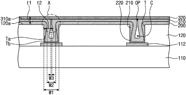
1. A semiconductor device, comprising:
a dielectric layer;
a trench formed in the dielectric layer;
a metal pattern that conformally covers a top surface of the dielectric layer, an inner side surface of the trench, and a bottom surface of the trench;
a first protection layer that conformally covers the metal pattern; and
a second protection layer that covers the first protection layer,
wherein a cavity is formed in the trench, the cavity being surrounded by the first protection layer,
wherein the first protection layer has an opening that penetrates the first protection layer and extends from a top surface of the first protection layer to the cavity, the opening being connected to the cavity, and
wherein a portion of the second protection layer extends into the opening to fill the opening so that at least a portion of the cavity remains in the trench.
|