| CPC H01L 23/562 (2013.01) [H01L 23/3128 (2013.01); H01L 23/49811 (2013.01); H01L 23/49822 (2013.01); H01L 23/49838 (2013.01); H01L 24/32 (2013.01); H01L 24/73 (2013.01); H01L 2224/32225 (2013.01); H01L 2224/73204 (2013.01)] | 20 Claims |
|
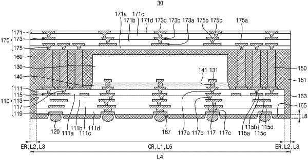
1. A semiconductor package comprising:
a semiconductor chip;
a lower redistribution layer under the semiconductor chip, the lower redistribution layer comprising a lower insulating layer and a trench, the lower insulating layer at a central region of the semiconductor package and at a portion of an edge region of the semiconductor package, the trench at a remaining portion of the edge region;
a plurality of outer connecting terminals under the lower redistribution layer;
a molding layer comprising a first molding section and a second molding section, the first molding section being on the lower redistribution layer and surrounding a side surface of the semiconductor chip and the second molding section being in the trench and contacting a side surface of the lower insulating layer; and
an upper redistribution layer on the molding layer,
wherein an outer side surface of the lower insulating layer and a side surface of the second molding section are coplanar with each other.
|